保护放大器输出免受过载电压影响的电路
以下为文章全文:(本站微信公共账号:cartech8)

汽车零部件采购、销售通信录 填写你的培训需求,我们帮你找 招募汽车专业培训老师
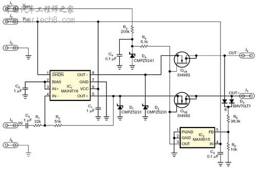
汽车电子产品的一个普遍要求是直接连接到配线装置,必须能够经得起电池电压的短路。虽然残酷,但这项规定对可靠性与安全来说是必要的。一个需要这种保护的例子是用于汽车内部产生间接噪声的音频放大器。虽然工作电压为3.3或5v,低于电池电压,但放大器必须能够忍受满电池电压。还可以使用适合其他汽车电路中放大器的保护网络 (图1)。一个双N沟道场效应管隔离从接线结点到另一端的高压条件的放大器输出。该场效应管,Q1A 和Q1B,通常情况下是开着的;齐纳击穿二极管D4及其偏置元件驱动场效应管的门限大约达到11V。双二极管D3提供OR二极管连接到每个输出的直流电压,从而产生电压控制分流调节器IC2的输出。电路保护IC1,1.4W的AB类放大器适于为汽车电子提供声音警告和指示。
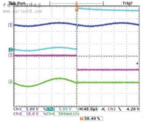
图1 适合其他汽车电路中放大器的保护网络 系统正常运行时,放大器输出的直流分量是VCC的一半——VCC为5V的情况下是2.5V。11V的门限驱动全面提升了 场效应管,而分流调节器的输出被关闭,因为它的反馈输入,第5脚,低于内部门限0.6V。如果输出超过5V,电流流经D3到R5/R6分压,拉动反馈端到其门限之上。然后分流调节器的输出拉着场效应管的栅极电压从11V接近地,关掉场效应管来阻塞放大器的高电压。场效应管很容易承受连续输出电压,当短路故障排除后,电路恢复正常运作。由于电路不能瞬间响应,齐纳击穿二极管D1 和D2在故障状态开始时提供了保护。 图2的波形显示了一个操作电路。放大器的输出之一(轨迹1)是一个偏置2.5V直流1kHz的正弦波。轨迹2是线束信号。它开始也是一个偏置为2.5V,1kHz的正弦波,但在200µs时,短接到一个18V电源上。 轨迹3是分流调节器的输出,最初偏置是11V,但被拉到地来响应过压状态。轨迹4是线束的电流。起初为正弦波,该电流在响应过载电压时降至零。
图2 波形显示了一个操作电路 图1的元件在5V时工作达到最优化。对其他电压值,可以调整的R5/R6的电阻值。分流调节器必须能够起饱和作用,因此除了逃避输出端外,还需要隔离电源管脚。该电路可以反复经受28V短路而不损坏。 英文全文: Circuit guards amplifier outputs against overvoltage An automotive-protection circuit withstands repeated insults of direct short circuits to the full battery voltage. John Guy, Maxim Integrated Products, Sunnyvale, CA; Edited by Charles H Small and Fran Granville -- EDN, 7/5/2007 A universal requirement for automotive electronics is that any device with direct connections to the wiring harness must be able to withstand shorts to the battery voltage. Though brutal, this requirement is necessary for reliability and for safety. One example of the need for this protection is an audio amplifier that produces indicator noises in the automotive interior. Though operating from a voltage of 3.3 or 5V, which is lower than the battery voltage, the amplifier must be able to stand off the full battery voltage. You can also use a protection network appropriate for these amplifiers for other automotive circuits (Figure 1). A dual N-channel MOSFET disconnects the amplifier’s outputs from the wiring harness in response to a high-voltage condition on either output. The MOSFETs, Q1A and Q1B, are normally on; zener diode D4 and its bias components drive the MOSFETs’ gates to approximately 11V. Dual diode D3 provides a diode-OR connection to the dc voltage on each output, thereby producing a voltage that controls the output of shunt regulator IC2. The circuitry protects IC1, a 1.4W Class AB amplifier suitable for audible warnings and indications for the automotive electronics. |
文章网友提供,仅供学习参考,版权为原作者所有,如侵犯到
你的权益请联系542334618@126.com,我们会及时处理。


会员评价:
共0条 发表评论